Facilities and capabilities
ASU resources
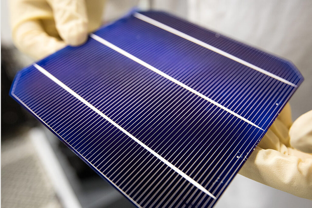
The laboratory area for the Solar Fab consists of 4,976 sq. ft. of class 100/1000 cleanroom space in the MacroTechnology Works building located in the ASU Research Park. It provides solar cell fabrication facilities for a broad range of materials, including silicon, III-V and thin film devices. These include an equipment set for pilot production of silicon solar cells that supports industrial size, single and multi-crystalline silicon solar cell fabrication for a range of silicon technologies, including silicon heterojunction, industry standard of AL-BSF. The pilot line has multiple capabilities for metallization, including screen print and copper plating. The facilities enable industrial interaction and fundamental growth and characterization studies for silicon III-V materials and novel structures relevant to photovoltaics.
In addition to fabrication of solar cells, the Solar Fab has facilities to turn the solar cells into modules, either small coupon modules for further testing or full-size modules. Testing for modules and reliability includes electroluminescence, environmental chamber and IV testing for outdoor modules. The encapsulation of solar cells is provided by an industrial size laminator capable of fabricating full size modules up to 1 m x 1.5 m or single cell coupons down to 1 cm². The provision of vacuum and controllable thermal cycling allows for the processing of a variety of materials including ethylene-vinyl-acetate and polyolefin.
Partial Equipment List
- Custom texturing hood
- Dedicated acid hoods
- MRL three-tube furnace
- AMI and MPM screen printers
- Fisher Scientific muffle furnaces
- AST RTA
- Veeco Gen III MBE
- Signatone four point probe
- Delta80BN spinner (SUSS MicroTec)
- KRUSS EasyDrop contact angle measurement system
- Nanometrics Nanospec AFT
- Rudolph AutoEl ellipsometer
- Hitachi S7800 CD SEM with EDS
- Alessi probe station
- Sinton FT250 cell flash tester
- Sinton lifetime tester
- Custom PL/EL tester
- PV Measurements QEX10 quantum efficiency system

Georgia Tech’s Resources
Processing: Dedicated wet benches, APCVD (PSG, BSG, SiO2), POCL3, Oxidation, LPCVD Polysilicon (undoped, boron and phosphorous), PECVD amorphous silicon, Low and high frequency SiNx & SiO2 deposition by PECVD, dielectric evaporators (ZnS, MgF2, Al2O3).
Metallization:Screen printing of Ag, Al and dopant and barrier pastes, metal evaporators (Ti, Pd, Ag, Al), electroless plating of Ag, photolithography tools such as mask aligner, green laser (via formation, cutting, doping), RTP, belt furnace, forming gas anneal tube.
Modeling & CharetricationTools: GIT has extensive capabilities and experience in characterization and analysis using tools such as light and dark I-V, C-V, Correscan, surface reflectance, QE, QSSPCD bulk lifetime, FTIR, LBIC, PL, ellipsometry, SEM, TEM, XPS.
Facilities: GIT PV programs have full access to the advanced semiconductor capabilities located in the microelectronics and nanotechnology centers on campus.

The following table lists the specific resource and capabilities at GIT.
| Process description | Equipment name and description | Model category | Name of model and description of parameters modeled |
|---|---|---|---|
| Wet Processing | Falcon Wet Bench VL clean hood, VL Texturing hood | PV Cost | E-cost (Calculates cost of electricity system) M-Cost 1 (Excel) and M-Cost 2 (MatLab) (Determines manufacturing cost of PV module) |
| Conventional thermal processing | SCHMID APCVD (BSG, PSG, Al2O3, SiO2) Centrotherm POCl3 & CTO MRL POCl3 & Boron Centrotherm: POCl3, Anneal Polysilicon deposition (PECVD & LPCVD) | PV Systems | Sizing PV Form PC Cad Size PV PV Design Pro GT PV Sim (Design and performance of PV system) |
| Dielectric deposition | Centrotherm PECVD SiN, SiO Dielectric Evaporator (ZnS, MgF2) ALD (Al2O3) | AR modeling | Sunrays and PV Optic ARCOAT Fresnel (Design and optimization of AR coating) |
| Metallization | Screen Printer with Automatic Alignment Screen Printer with Manual Alignment Green Laser (vias, cutting, doping) Metal Evaporator (Ti, Pd, Ag, Al) Photolithography Bay Mask Aligner | Grid Optimization/ Process Modeling | Grid Design (Design of front contacts) SSuprem3 (1-D process simulator) SSuprem4 (2-D process simulator) |
| Contact formation | Despatch contact firing Belt furnace Custom RTP/RTA Plasma Edge Isolation System Forming Gas Anneal Furnace Plating Wet Bench | Device modeling | Dessis (2,3-D device modeling) Quokka 2D modeling PC1D (1-D device modeling) S-model (Surface passivation modeling) Jo (Computes reverse saturation current) SRV (Calculates effective surface recombination velocity for varying passivation) PCD (Computes lifetime coefficients from PCD measurements) Lifetime (Models SRH lifetime in bulk silicon) IQE (Analysis of IQE, Leff, SRV, and light trapping) |
| Tools to characterize finished cells | FTIR SEM/TEM IQE XRD LBIC Opticalscope Correscan IV Tester (Dark & Light) Solar Simulator Suns Voc Testers Surface Charge Analyzer QSSPCD lifetime testers | Device modeling | (Same as above) |